


CHAIRPERSON
Hence the R&D line for OSAT in co-packaged optics space and a system for networking domain will be a true silicon-to-system from Kaynes Semicon.
Managing Director
We will bring experienced OSAT leaders from southeast Asia and Taiwan, and create an ecosystem of trained engineers, operators and technicians for India.
SENIOR VICE PRESIDENT - ENGINEERING
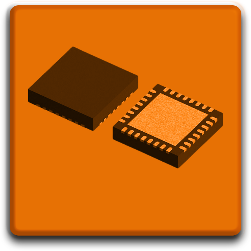
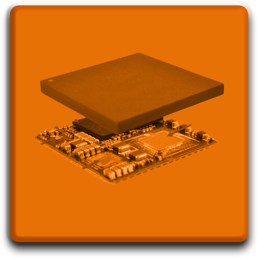
Our Test Roadmap and CapEx spending will cover Analog, Digital Mixed Signal, RF, Power, Memory and modules which will allow Kaynes to test from legacy packages to advance 3D and SiPh packages.

HEAD OF R&D
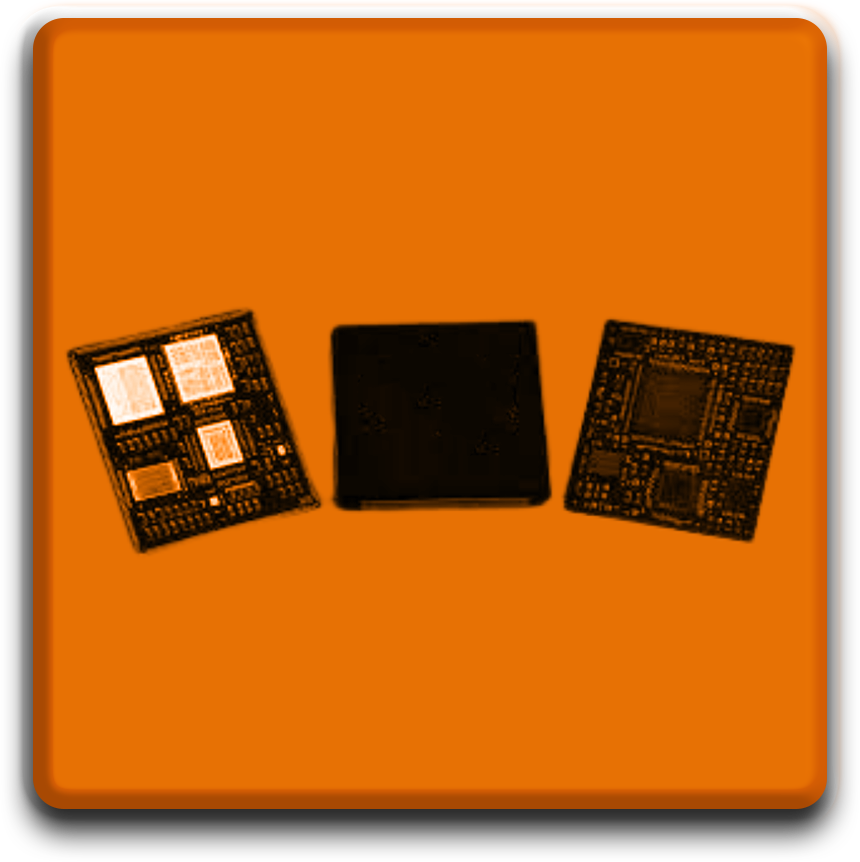
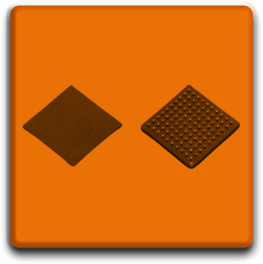
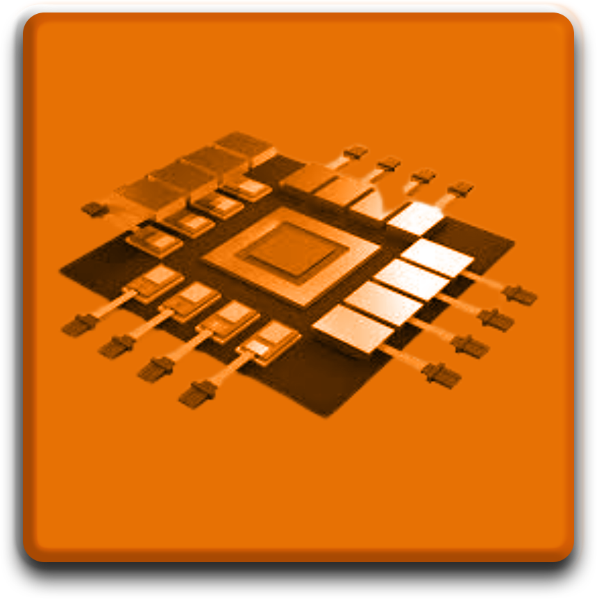
Joining Kaynes Semicon in its foundational phase in 2024 means being part of something truly exciting. We're not just building a facility; we're architecting a global leader in advanced packaging from the ground up. Our R&D is laser-focused on mastering and advancing the innovative technologies, including 2.5D/3D integration, chiplet strategies, and other cutting-edge packaging solutions, that will define that leadership.

HEAD OF NEW BUSINESS
At Kaynes Semicon, we are not just building facilities, we are building futures. By integrating global expertise with local talent, we aim to position India as a strategic hub for OSAT services and advanced semiconductor manufacturing.
Hence the R&D line for OSAT in co-packaged optics space and a system for networking domain will be a true silicon-to-system from Kaynes Semicon

We will bring experienced OSAT leaders from southeast Asia and Taiwan, and create an ecosystem of trained engineers, operators and technicians for India
From its first OSAT plant, the company is primarily looking to serve automotive electric vehicle (EV) and industrial segments. The plant will have a couple of chip assembly lines. "In the EV domain, we will be focussing on power modules pack- aging. The second vertical we will go after is industrial, where we will look after micro-controller units (MCUs).
Our Test Roadmap and CapEx spending will cover Analog, Digital Mixed Signal, RF, Power, Memory and modules which will allow Kaynes to test from legacy packages to advance 3D and SiPh packages
Joining Kaynes Semicon in its foundational phase in 2024 means being part of something truly exciting. We're not just building a facility; we're architecting a global leader in advanced packaging from the ground up. Our R&D is laser-focused on mastering and advancing the innovative technologies, including 2.5D/3D integration, chiplet strategies, and other cutting-edge packaging solutions, that will define that leadership.
At Kaynes Semicon, we are not just building facilities, we are building futures. By integrating global expertise with local talent, we aim to position India as a strategic hub for OSAT services and advanced semiconductor manufacturing.